- Uncompromised characterization of all types of materials at the nanoscale
- Ideal for characterization of materials at low beam energies for maximum surface topography
- Excellent imaging of beam-sensitive and non-conductive samples
- Fully automated setup of electron beam – optimal imaging conditions are guaranteed by the In-Flight Beam Tracing™
- Intuitive live SEM navigation on the sample at magnification as low as 2× without the need of extra optical navigation camera thanks to the Wide Field Optics™ design
- Unique In-Beam Multidetector design allowing angle and energy selective BSE detection
- Intuitive software modular platform designed for effortless operation regardless users’ skill level
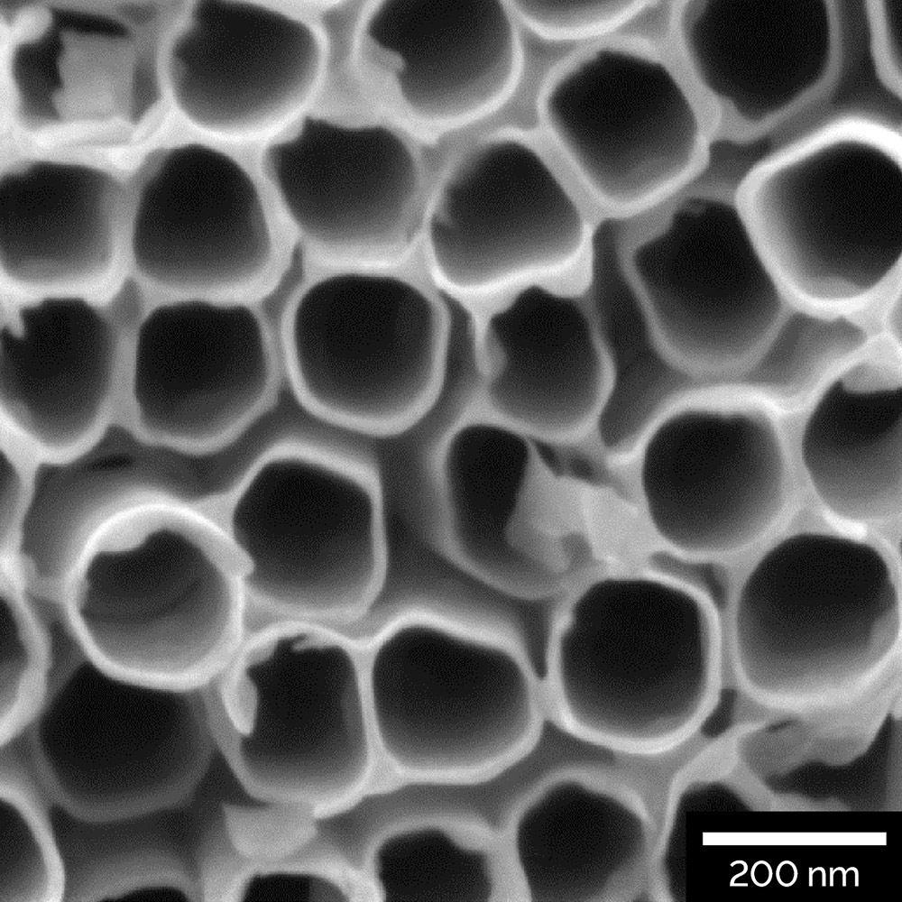
- Ti Nanotubes
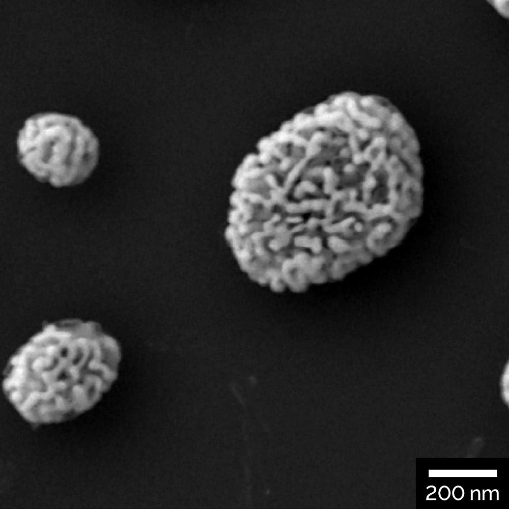
- Nanoporous gold on Si
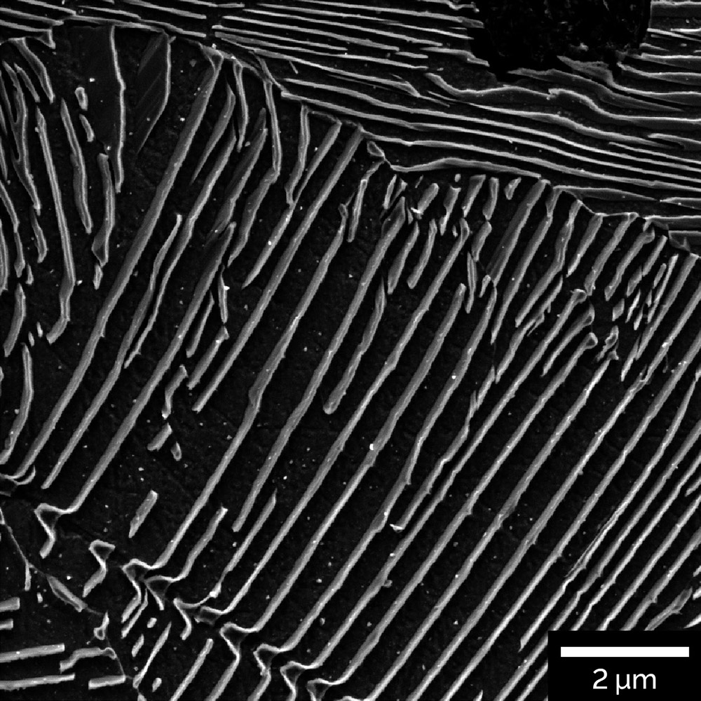
- Interlamellar spacing in perlite of cast iron


